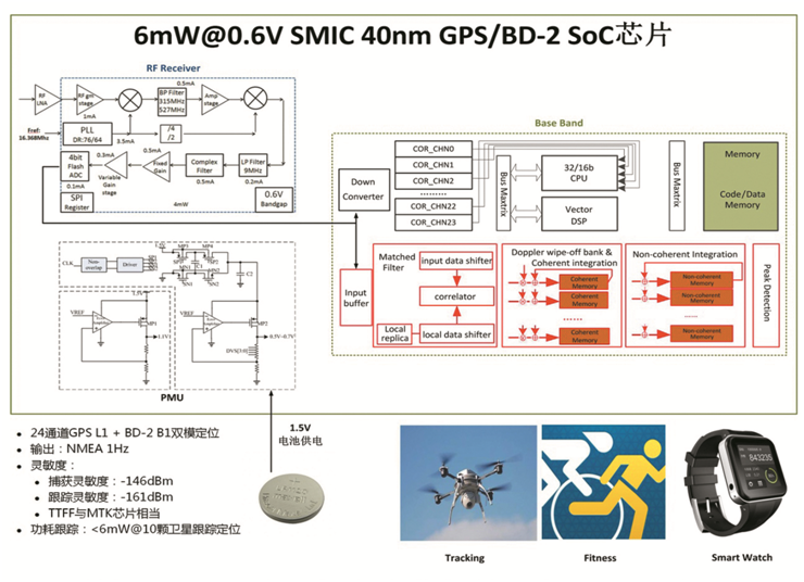
In current market, the power consumption of GNSS chips are usually larger than 10mW, so that they are not suitable for wearable or IoT products. Nation ASIC System and Engineering Research Center has designed a GNSS SoC chip with a power consumption of less than 6mW when tracking 10 satellites, a position accuracy of 3m CEP, and an acquisition sensitivity of -146dBm. Key innovations of our design are: 1) an ultra-low power parallel tracking architecture and an acquisition engine using a partial matched filter and a multi-stage Doppler mixer; 2) an ultra-low power digital PLL and a new structure of the mixer able to solve the problem of lower voltage margin; 3) a memory structure using near-threshold voltage which is tolerant to process variation to provide stable read and write operations; 4) a high accuracy and low voltage standard-cells library.


